By Loyd Case, PCWorld
- Sep 13, 2012 6:00 AM
PC users on the go require long battery life, but don’t want to sacrifice performance. Balancing these contradictory requirements are at the heart of Intel’s new CPU architecture, code-named Haswell, which is expected to appear in shipping tablets, ultrabooks and other computers in 2013.
At the 2012 Intel Developer Forum earlier this week, Intel dove deeper into what makes Haswell tick.
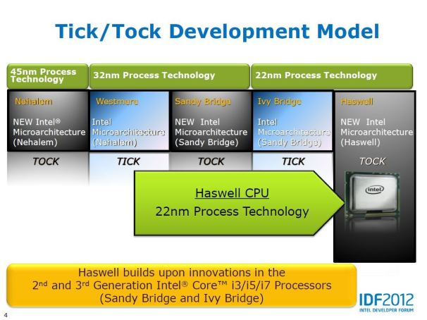
Or maybe "tock" would be a better word, as Haswell represents the "tock" in Intel’s CPU development program. Intel uses “tick-tock” to denote its CPU development strategy. A “tick” is represented by an existing CPU design that’s tweaked only a bit, but enjoys all the efficiencies of a new manufacturing process. Ivy Bridge represents a tick, incrementally improving on Sandy Bridge, but moving to 22nm. New architectures like Haswell, meanwhile, are always built on proven manufacturing processes, and Intel’s 22nm manufacturing process has been well shaken out thanks to the company’s Ivy Bridge line. So Haswell represents a “tock.”
 Haswell is a "tock"
Haswell isn’t just another Intel PC processor, though. Intel is talking about Haswell-based processors ranging from dual-core chips running at less than 10 watts (making them suitable for tablets) to quad-core desktop CPUs that can out-perform the fastest Ivy Bridge processors. Just how did Intel hit its aggressive target of 20x improvement in power efficiency? It’s worth looking at Haswell’s power management tech before diving into the CPU proper.
Sleepily Active
Modern CPU power management involves cutting power to large chunks of the processor when it makes sense to do so, based on whatever tasks you’re asking your device to do. Intel can manage power almost to the transistor level by using a special processing unit built directly inside the main CPU–Intel calls it the Power Control Unit. The PCU looks at which parts of the processor aren’t being used, and can turn individual parts on and off as needed.
The problem, though, isn’t putting parts of the CPU to sleep. The problem is waking up the processor fast enough to be useful. After all, if you had to wait a minute every time your laptop went to sleep, you’d probably throw it against the wall in frustration. Intel CPUs up to Ivy Bridge have had two main states: active and sleep. (It’s more complicated than that, but that’s the general idea.) Over the years, Intel has steadily decreased the amount of time it takes to wake a sleeping CPU. The current Ivy Bridge processor takes several seconds to wake up from a deep sleep state. Several seconds is still not quite "instant on" though.
The solution in Haswell is to add a third power state, something Intel designers call "Active Idle." Active Idle, also labeled SOix, is an extremely low-power active state that uses 20 times less power than Ivy Bridge. The PC system itself thinks it’s awake, but the CPU is still mostly asleep. This trick translates into wake times of, at worst, a few hundred milliseconds. A worst-case wake up time of a half second is considerably better from the user perspective than the several seconds current CPUs take to wake up. Haswell is almost always in this "instant resume" state when running. Much of the tech was borrowed directly from Intel’s Atom processor power management.
 Haswell power management improvements
Intel used a few other tricks in building Haswell. Earlier, we talked about idle and sleep states. The sleep and Active Idle states are actually divided into multiple smaller states. Each mini-state (known as "C-states") defines exactly what part of the CPU is turned off. Haswell adds new C-states for more granular power management. This delivers longer battery life because your CPU won’t constantly be waking up a part of the CPU it doesn’t need in order to wake up some part of the CPU it does need.
Intel also took a look at how CPU power usage interfaces with a system’s display. Indeed, one thing that takes a long time to wake up in today’s systems are LCD panels, so Haswell processors will include panel self-refresh. So, for example, if you’re just sitting there staring at your screen, a Haswell CPU will go to sleep, with only a tiny part staying awake to refresh the monitor. As soon as you move the mouse or press a key, the CPU wakes up. You don’t notice the wake-up time, because the display never went to sleep.
Now that you’ve seen a bit of how Intel achieved better power efficiency, let’s talk about CPU architectural enhancements.
More Performance, Better Power Efficiency
During one of the IDF technical sessions, Intel Senior Principal Engineer Ronak Singhal repeated several times that no new feature was added to the CPU if it introduced a power penalty. Even so, there are a number of tricks CPU designers have up their sleeves to improve performance while balancing power needs.
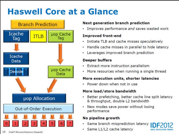
One trick is branch prediction, which lets the CPU peek ahead to see which instructions are likely to be executed in the near future. If the CPU knows which instructions will be coming down the pipeline, it can be much more efficient about allocating CPU resources, turning on only parts of the CPU that are needed. So Intel tweaked architectural elements to improve branch prediction, including bigger internal buffers and larger out-of-order windows.
 Haswell CPU core block diagram
Also, the more work a CPU can do in a single cycle, the better the performance at the same power usage. So Intel added the ability to do two floating point multiply-adds every clock cycle, doubling the performance throughput over Ivy Bridge for the same power usage. The L1 and L2 cache throughput has also been improved, lowering the time taken by the CPU to wait for data to arrive.
Of course, none of this good stuff comes free. While power efficiency has improved, it’s at the cost of chip real estate. Given that Haswell will still be built on 22nm, the chips themselves are likely to be larger than Ivy Bridge CPUs.
The chip size is likely to increase for another reason as well: graphics.
High End PC Gaming on Tablets: Haswell Graphics
Haswell builds on the existing Intel HD graphics core in Sandy Bridge, mostly adding refinements and improving power efficiency. Haswell now offers three different integrated graphics options for Intel CPUs, called GT1, GT2 and GT3, as opposed to the two options (Intel HD 2500 and HD 4000) available with Ivy Bridge.
GT3 is the most interesting version from a performance perspective. GT3 doubles the performance over the older HD 4000 GPU by simply doubling the number of execution units. Execution units are the core computation engine of the GPU, handling graphics shader and GPU compute tasks. These execution units are built into a common modular unit, which Intel calls a “slice common.”
The slice common also includes a number of other key components for real time graphics, such as the raster engines and cache. To double the number of compute engines over HD 4000, Intel simply added a second slice common to GT3. This takes up additional chip space, but actually saves power, since the GPU doesn’t need to enter turbo mode for additional performance.
There are other tweaks to the GPU as well, including improvements to texture samplers, improving overall bandwidth and adding more circuitry to take up tasks that’s currently handled by the driver in the current HD 4000.
These features all serve to increase performance without increasing power consumption. Intel estimates that an 8W Haswell unit could conceivably integrate a full GT3 GPU, though no specifics on product versions were given. Intel showed two different applications running: Unigine Heaven, a synthetic graphics benchmark and Bethesda’s Skyrim, a PC RPG with demanding graphics requirements. Haswell ran both tests at double the performance of Ivy Bridge, creating a much smoother visual experience.
Historically, Intel has also been late to the party in adding software support for the latest programming interfaces. Haswell changes this by implementing all the latest standards: DirectX 11.1 for Windows 7 and Windows 8, OpenCL 1.2 for GPU compute and OpenGL 4.0. Intel’s been good about driver support, offering both Windows and Linux drivers.
While Haswell’s 3D graphics engine is substantially improved over past Intel efforts, desktop PC users will likely still want high-end discrete graphics cards for best PC game performance. But Haswell’s graphics core will make extremely thin Ultrabooks respectable gaming platforms, and the new GPU opens up possibilities for modern PC games running on Haswell-based tablets.
The Video Engine
Ivy Bridge introduced the QuickSync video block, a dedicated, fixed function video unit built into the GPU. Building a fixed function video engine enables much faster video encode and decode performance. The downside is that it’s not programmable, so if some hot new HD codec came along, the video engine couldn’t handle it. Given that video codecs are pretty standardized, that’s not likely.
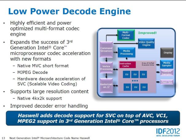
 Haswell video engine details
However, Intel did add additional codec support to the Haswell video engine. Motion JPEG (MJPEG) is important for video conferencing. SVC, or scalable video codec, is useful in mobile environments, where the quality of the video may change depending on the speed of the connection, so the video quality can scale gracefully. Users will still see good frame rates instead of jerky or dropped frames if network bandwidth degrades. Support for 4k video for the upcoming generation of ultra-high definition panels was also added.
 Haswell running 4k x 2k video on an ultra high-def display
Bottom line: bigger chip, better performance, lower power
Haswell will take up more die space than Ivy Bridge, which translates to a higher cost-per-CPU for Intel, since it won’t be able to build as many Haswell CPUs on a single wafer. However, this is somewhat mitigated by Haswell’s modularity, which will let Intel build many different Haswell products, targeting lower power niches with smaller versions. Even better, Haswell is positioned well for Intel’s next generation 14nm manufacturing process.
Most of the performance tweaks to the main CPU are evolutionary when compared to Ivy Bridge. At the same clock frequency, users may see performance improvements of up to 10%. The big gains are in power efficiency and graphics performance. The improvements in power efficiency will enable laptops finally hitting all-day battery life in Ultrabooks, while GPU improvements will mean mobile users will have reasonably robust game experiences on the go.
Haswell looks to be the CPU with the biggest potential impact on Intel’s bottom line of any CPU in years. The wide range of products enabled by the new CPUs modular nature and power efficiency will likely see Haswell products in a wide array of form factors. Users will benefit by having more choices than ever in mobile and desktop form factors, with improved performance and longer battery life.
ORIGINAL SOURCE: http://www.pcworld.com/article/262241/inside_intels_haswell_cpu_better_performance_all_day_battery.html